
Interactive electronics resource
Logic Gate Board Instructions
Build, understand and experiment with the Logic Gate Board. This resource brings the original kit material into the current MitchElectronics format with the schematic, circuit explanation, component and PCB information, construction guidance, troubleshooting and practical ideas where available.
Introduction
What are logic circuits?
Before we can understand what logic circuits are, we first need to understand the difference between digital and analogue circuits.
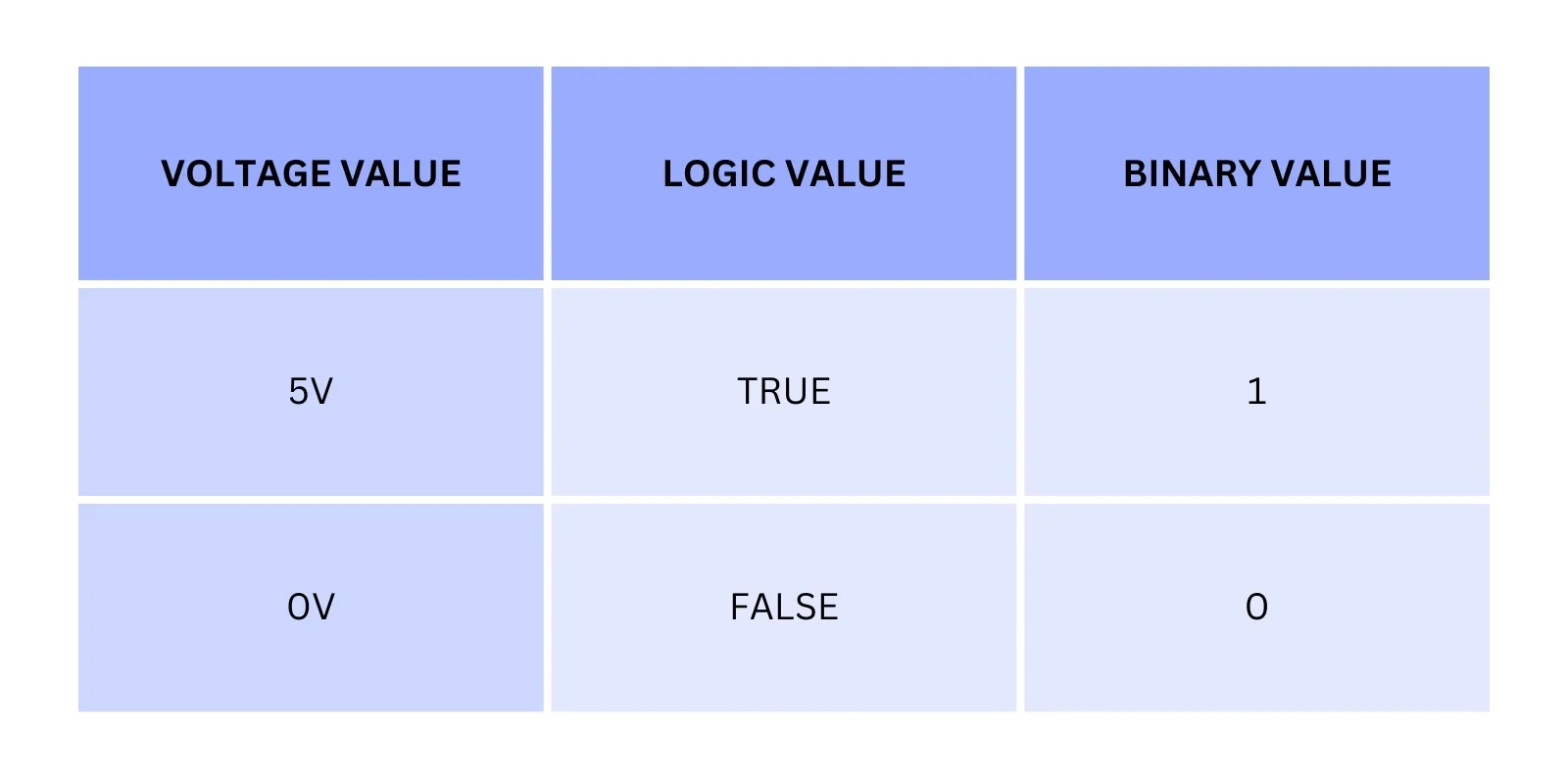
Analogue circuits are those whose voltages can be any continuous value, such as 5V, 3V, and 1.5V, and such circuits can be found in various MitchElectronics kits, including the Simple Function Generator, the 555 astable and monostable kits, and the discrete op-amp kit. Digital circuits, however, are those that use two specific voltage levels, such as 5V and 0V, with one representing true (a binary 1) and the other representing false (a binary 0).
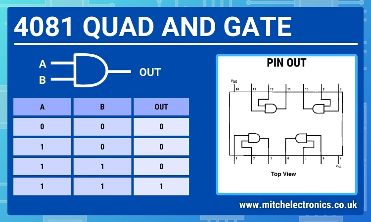
Circuits that process digital signals to compute logical functions are known as logic circuits. For example, the logic function AND produces a logical 1 output when all inputs to the AND gate are a logical 1 (more on this later), otherwise the output will be a logical 0.
The overwhelming majority of logical circuits use 0V as the false value (or binary 0), but the voltage for a true signal depends on the power supply of that circuit. Common values for the logical value of true (or binary 1) include 5V, 3.3V, and 1.2V, and in MitchElectronics kits, a true value is defined as 5V.
Glue logic and logic families
Logic gates are the fundamental building block of any logic circuit, and are found in almost all electronic devices. While modern devices such as CPUs integrate millions of logic gates onto a single chip, the first logic devices had to rely on sticking individual logic gates together using wires, which was (and still is) known as glue logic.
Creating logic gates can be done using discrete transistors, but such a design gets extremely large very fast (early computers in the 50s made using this technology would take up entire rooms). Instead, we can use discrete logic chips that integrate a few gates, helping to reduce the size of designs.
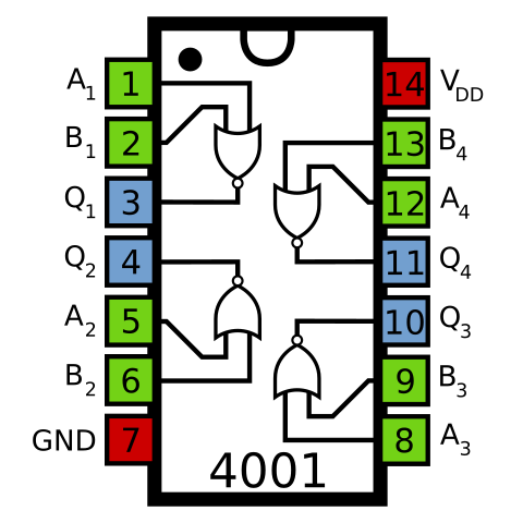
The two most common (and famous) family of logic chips are the 7400 series (introduced 1966) and the 4000 series (introduced 1968), which include numerous logic functions such as AND gates, NAND gates, flip-flops, shift registers, and even full adders. The 7400 series of chips came out before the 4000 series and originally utilise TTL logic, whereas the 4000 series utilised CMOS logic.
Early designs preferred the 7400 series due to its faster speeds, but as CMOS technologies improved (offering both speed and low energy consumption), it didn’t take long for the 7400 series to introduce CMOS versions. In fact, the benefits that the 7400 series and 4000 series provide still justifies their manufacture even till this day.
What is the Logic Gate Board?
Both the 7400 and 4000 series costs of hundreds of chips, with each one being useful in its own right. However, trying to learn what each chip does is completely useless as most will rarely be used in modern designs. Instead, it is better to learn how the most crucial chips work, so that you can readily use them in projects.
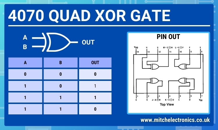
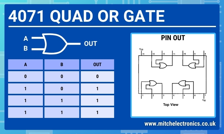
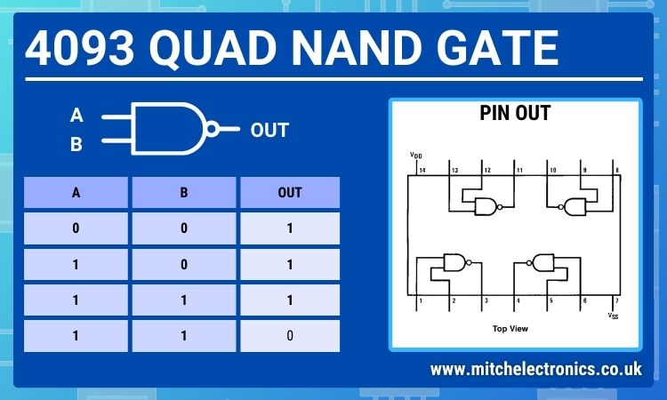
The Logic Range of kits, including the Gate Board, is designed to help you understand and learn how to use these chips by providing the various inputs and outputs needed to drive them. In the case of the Gate Board, this kit will allow you to test some of the most crucial logic gate chips; the 4001, 4070, 4071, 4081, and 4093.
Schematic
How does the logIC gate board work?
The chips
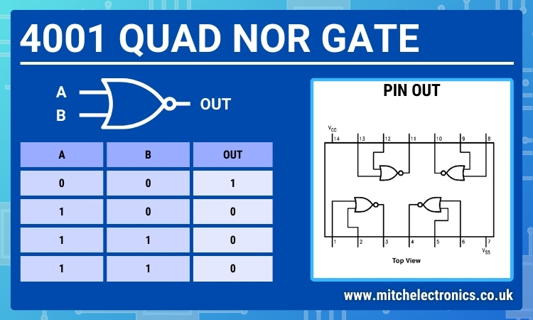
The Gate Board is designed to allow you to test AND, NAND, NOR, OR, and XOR gates utilising the 4001, 4070, 4071, 4081, and 4093 ICs. The board itself only has one DIP socket, meaning that only one chip can be tested at a time, and because each of these chips has the same pinout, no changes to the board need to be made.
Each of these chips is a 14-DIP IC that house 4 identical logic gates, and each of these logic gates has the same pin locations for each gates inputs and outputs, allowing the chips to be swapped with ease (of course, the logic function is different). The reason why this kit doesn’t allow for testing a NOT gate chip is because there are no NOT gate ICs in a 14 DIP package following the same pinout, but a NOT gate can be realised with the NAND and NOR ICs via the second sub-circuit (see The Board for more details).
The board
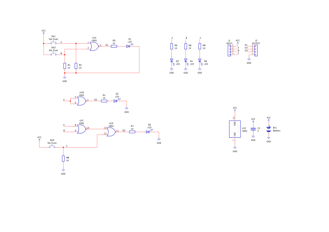
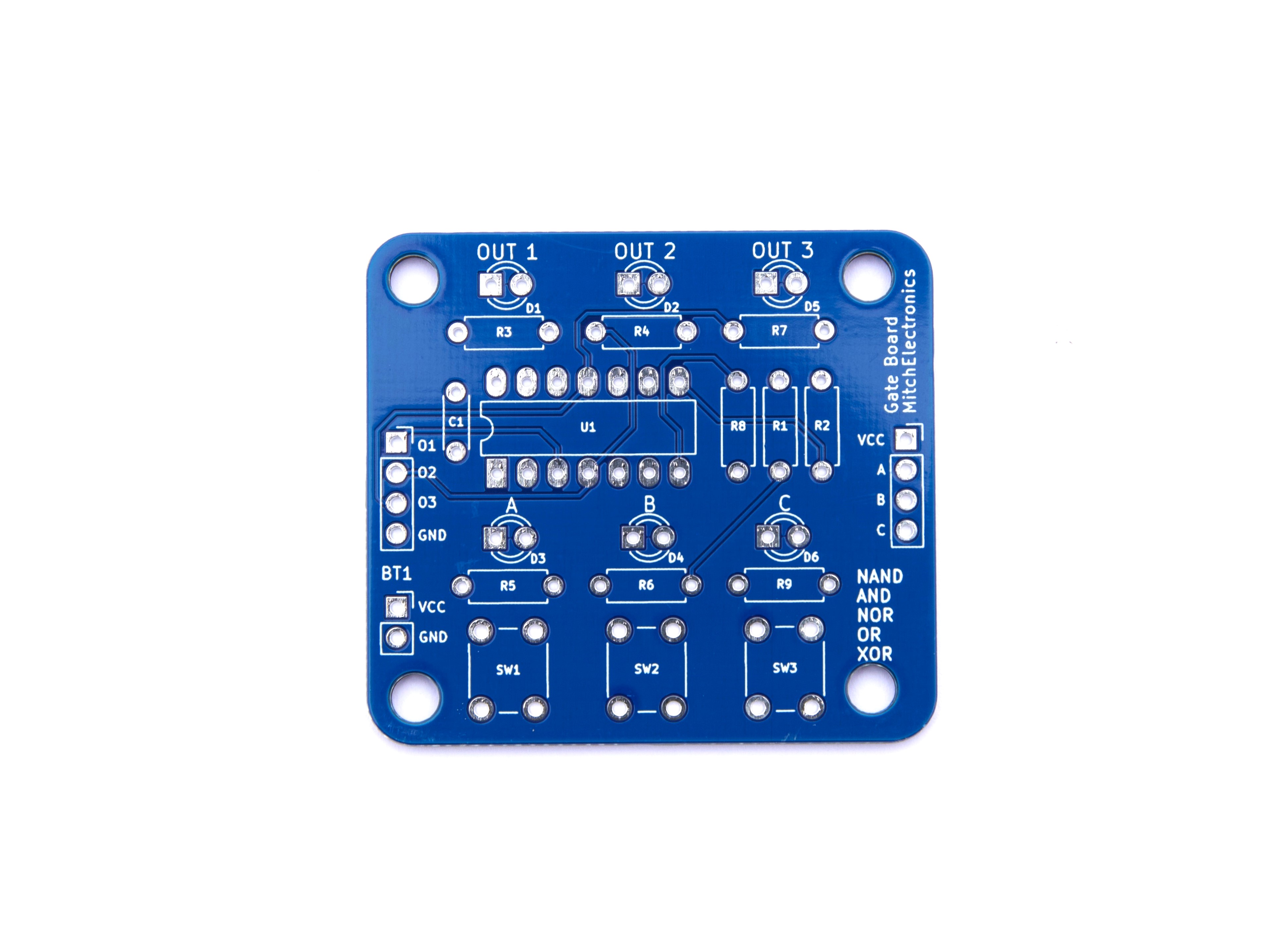
The Gate Board integrates three input buttons, three input LEDs, and three output LEDs, which allow for the testing of various logic gates, and the entire board is split into three main logic sub-circuits. The first sub-circuit, indicated by the output LED A, allows the logic gate to be tested independently with the two switches A and B being connected into its inputs.
The second sub-circuit, indicated by the output LED B, allows the logic gate to be tested with a single switch, A, where both inputs are connected together. The final sub-circuit, indicated by the output LED C, allows for a combination of two gates to be tested, with all three switches providing inputs to this circuit.
On the sides of the board are further expansion connectors that you can use with other Logic Range kits. However, instead of providing connections to each logic circuit, only the inputs and outputs are provided on these pins.\
Try it yourself
Circuit simulation
Not available in mobile view
What you need
Component List
| Component | Quantity | PCB Reference |
|---|---|---|
| 14 DIP Socket | 1 | U1 |
| 100nF Capacitor | 1 | C1 |
| 1K Resistor | 9 | R1 to R9 |
| 3mm Red LED | 6 | D1 to D6 |
| Tactile Switch | 3 | SW1, SW2, SW3 |
| 4001 | 1 | U1 |
| 4070 | 1 | U1 |
| 4071 | 1 | U1 |
| 4081 | 1 | U1 |
| 4093 | 1 | U1 |
| PP3 Connector | 1 | BT1 |
| Logic Board PCB | 1 | — |
Inspect the board
Interactive BOM
Board reference
PCB & assembly
The PCB silkscreen and component references should be checked against the component list before soldering each part.
Before applying power
- Check every component against its PCB reference.
- Confirm the orientation of all polarised components and ICs.
- Inspect for solder bridges, unsoldered pads and clipped leads that could cause a short.
- Check that no loose wire or solder debris remains on the board.
Build with confidence
Construction tips
Recommended build order
A reliable way to assemble Logic Gate Board is to work from the lowest-profile components to the tallest. This keeps the PCB easy to access while you solder.
- Fit resistors, links and other low-profile components first.
- Fit small capacitors and diodes, checking polarity where applicable.
- Fit IC sockets and small semiconductors, observing the orientation markings.
- Fit larger capacitors, potentiometers, switches and other controls.
- Fit LEDs, connectors and the remaining taller components.
- Insert socketed ICs only after soldering around the socket is complete.
- Inspect every joint and check for solder bridges before applying power.
Electronics construction guidance
If you are new to kit construction, use the Soldering Guide alongside these instructions. Identify each component before fitting it and compare its reference with the component list and PCB silkscreen.
When it does not work
Troubleshooting
Nothing happens when power is applied
- Confirm the supply is connected to the correct input and with the correct polarity.
- Check that ICs, diodes, LEDs, transistors and electrolytic capacitors are fitted in the correct orientation.
- Compare component values and positions against the component list and PCB reference.
- Inspect for missed joints, dry joints and accidental solder bridges.
The circuit powers up but does not behave as expected
This kit is intended for 4000-series logic gate experimentation. If the output is stuck, unstable or outside the expected behaviour, use the schematic to trace the circuit a stage at a time rather than replacing several parts at once.
Check the components around the part of the circuit responsible for the output or timing first. A misplaced resistor, reversed semiconductor or poor connection can allow a circuit to power up while preventing it from operating correctly.
The circuit works intermittently
Intermittent behaviour is often caused by a marginal solder joint, a loose connector or a component lead that has not been fully soldered. Gently inspect the board with power removed and reflow any joint that looks dull, cracked or incomplete.
If the fault remains, compare the assembled board with the schematic and PCB reference one connection at a time.
Ready to test and experiment?
Use a signal generator to test how fast the logic circuits can respond to signals
Once the board is working, compare its behaviour with the schematic and the explanation above. Try changing only one input, control or permitted component value at a time so you can clearly see what effect that change has on the circuit.