


Before you learn how the 4013 D-Type Flip Flop Board works, you should first learn how the Logic Gate Board works as that kit covers the basics of logic. The Logic Gate Board kit also provides multiple logic chips in the 4000 series, demonstrating how these chips work and how some of the 4000 series share similar packages and configurations.
In electronics, it can often be important to remember the state of a signal so that it can be recovered at a later date. For example, it may be necessary to read an analogue voltage and store the value for signal processing that itself can take a while (commonly found in sample and hold circuits). Another example of where remembering a signal can be important is in a digital control circuit that needs to remember if a button has been pressed (such as the delay in an alarm system).
In the case of digital circuits, a latch is a device that can be used to remember the state of a logic signal, acting as form of memory (CPU cache memory uses such latches). Once a signal has been latched into the latch, the original signal can be removed, and the latch will still retain the value that it saw.
Latches are asynchronous devices, meaning that they will remember a signal as soon as they are presented with one, and they have two different inputs for remember either a 1 or 0 (often called set and reset). Such latches also have two outputs; one representing the remembered bit, and the other being the opposite of the remembered bit.
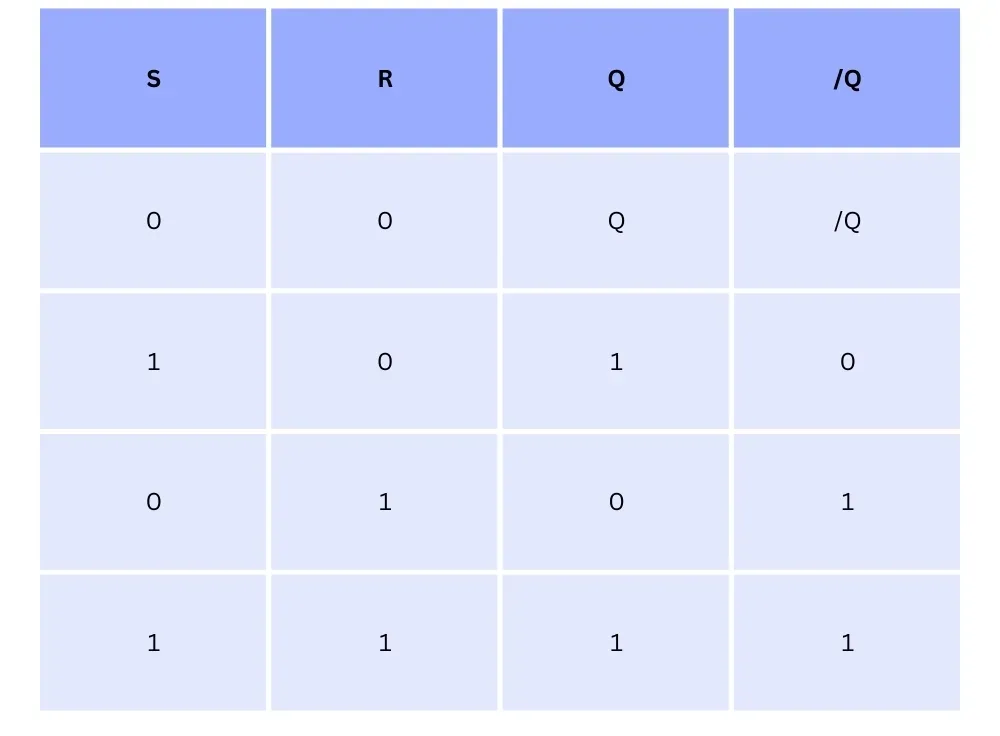
As such, latches have two possible states that they can be in, and if a logical 1 is presented to the set input, the latch will switch on (and stay on), and if a logical 1 is presented to the reset input, the latch will switch off (and stay off).
Latches are a critical circuit for digital electronics, but they are rarely used on their own. This is because latches suffer from a few issues, with the two biggest issues being that they latch their data immediately, and that they require two separate inputs for controlling the state of the latch.
To fix this issue, most latches are made synchronous using a few additional components, utilising a clock input for setting and resetting the data, and a single data input to set the value of the latch. Such devices are called flip-flops, and they make up the foundation of modern digital systems.
Because flip-flops are clocked devices, changes on the data input are completely ignored by the flip-flop if the clock input remains low. It is only when the clock input rises from a 0 to a 1 that the data present on the input sets the state of the flip-flop.
As the data input is a single bit, it also makes storing information far easier, but it also allows for some rather interesting configurations. For example, if the inverting output is connected to the data input, each clock pulse causes the flip-flop to flip its state (called a toggle).
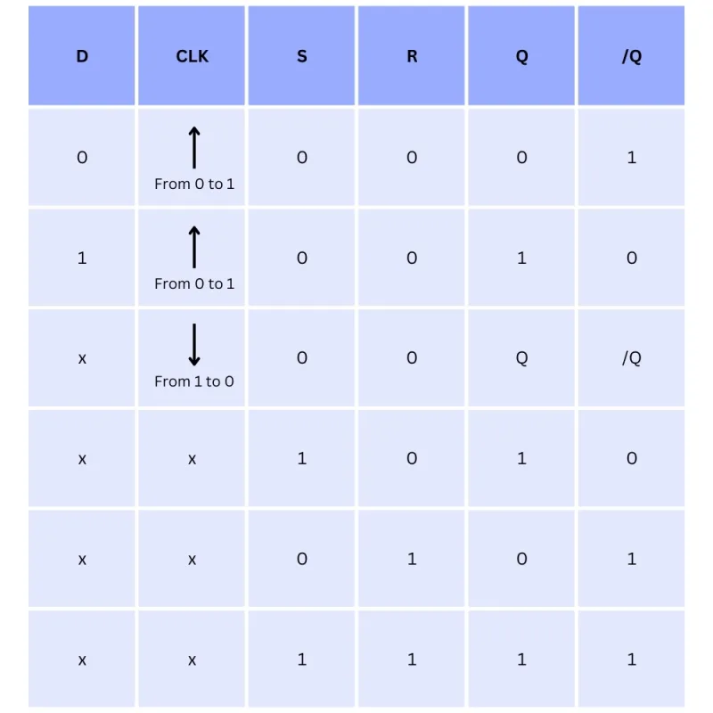
The 4013 D-Type Flip Flop kit is designed to let you experiment with the famous 4013 IC, which incorporates two independent flip flops. Each of these flip-flops not only has two complementary outputs, a clock input, and data input, but also a set and reset input that can be used to force the state of the flip-flop to a particular value.
Even though the 4013 IC (which is a part of the 4000 series of logic devices), has two independent flip-flops, the kit only uses one of these flip-flops, with the other being entirely used. This is to keep the circuit simple and reduce the number of components on the PCB.
The board integrates a special switch, SW3, which allows for connecting the D input to the complementary output /Q, which will turn the flip-flop into a toggle latch. When in toggle mode, pushing the clock input, the internal state of the flip-flop will switch to the opposite value.
| Component | PCB Reference | Quantity | Looks Like |
|---|---|---|---|
| 14 DIP Socket | U1 | 1 | 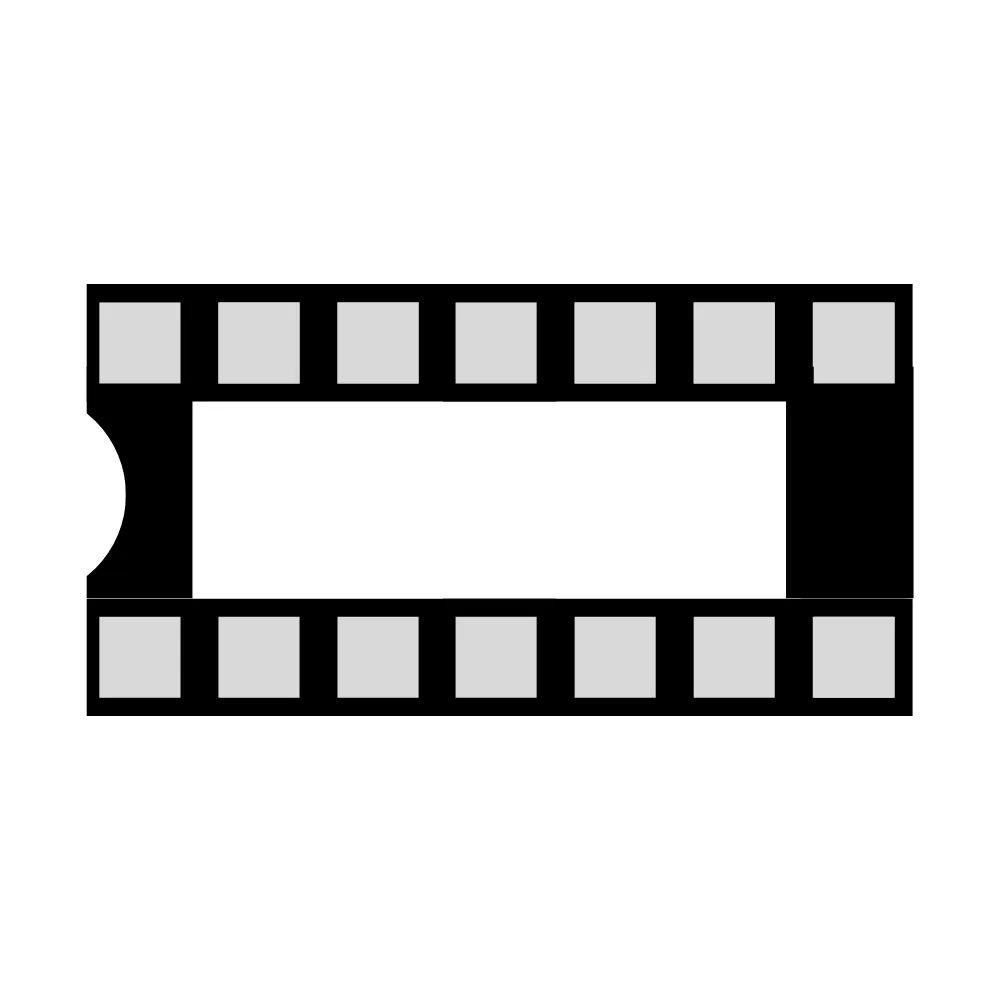 |
| 4013 Dual Flip-Flop IC | U1 | 1 | 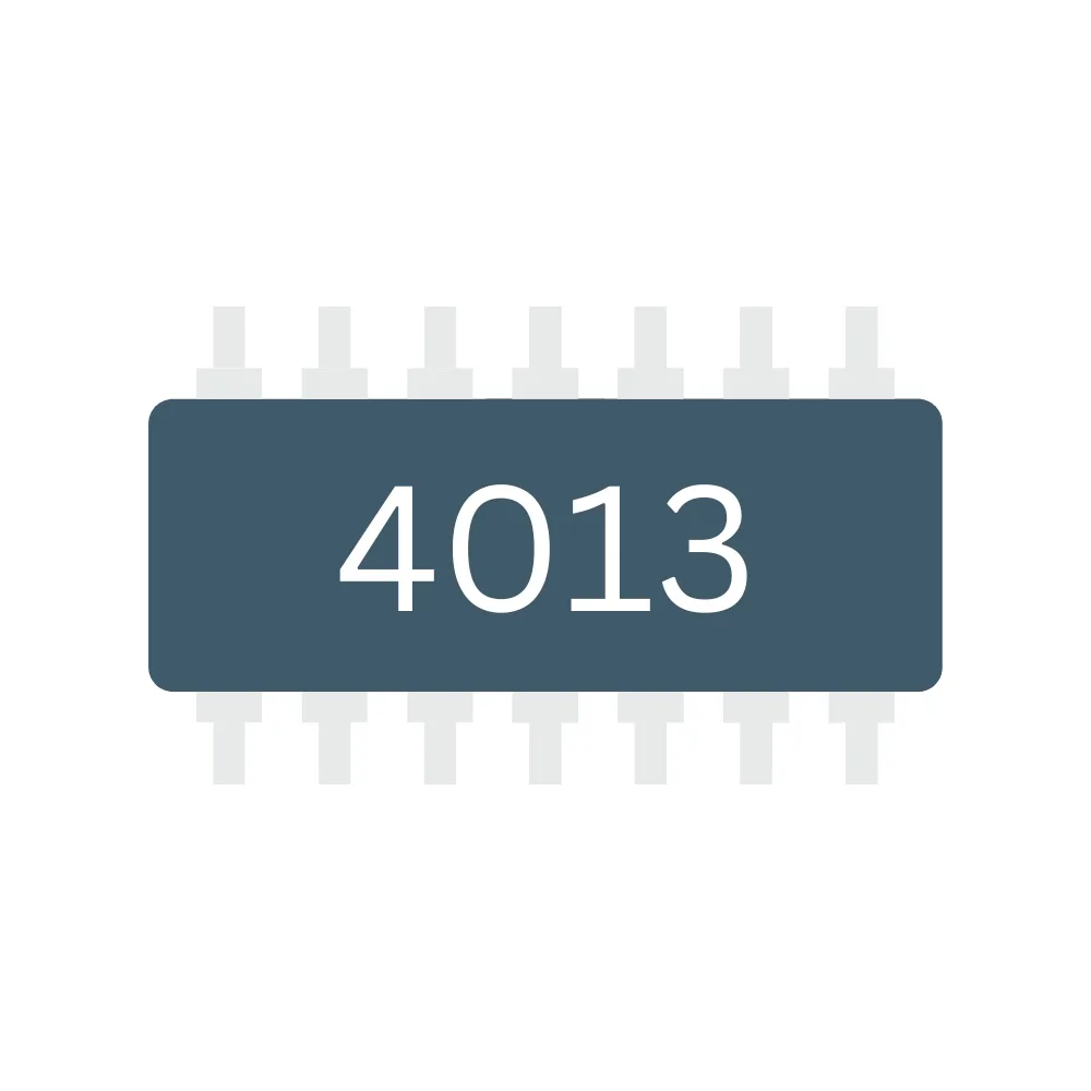 |
| 100nF Ceramic Disc Capacitor | C1 | 1 | 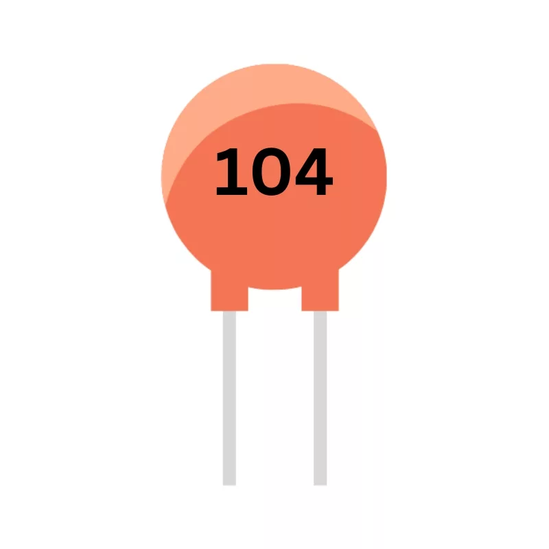 |
| 1K Resistor | R1, R10 | 10 | 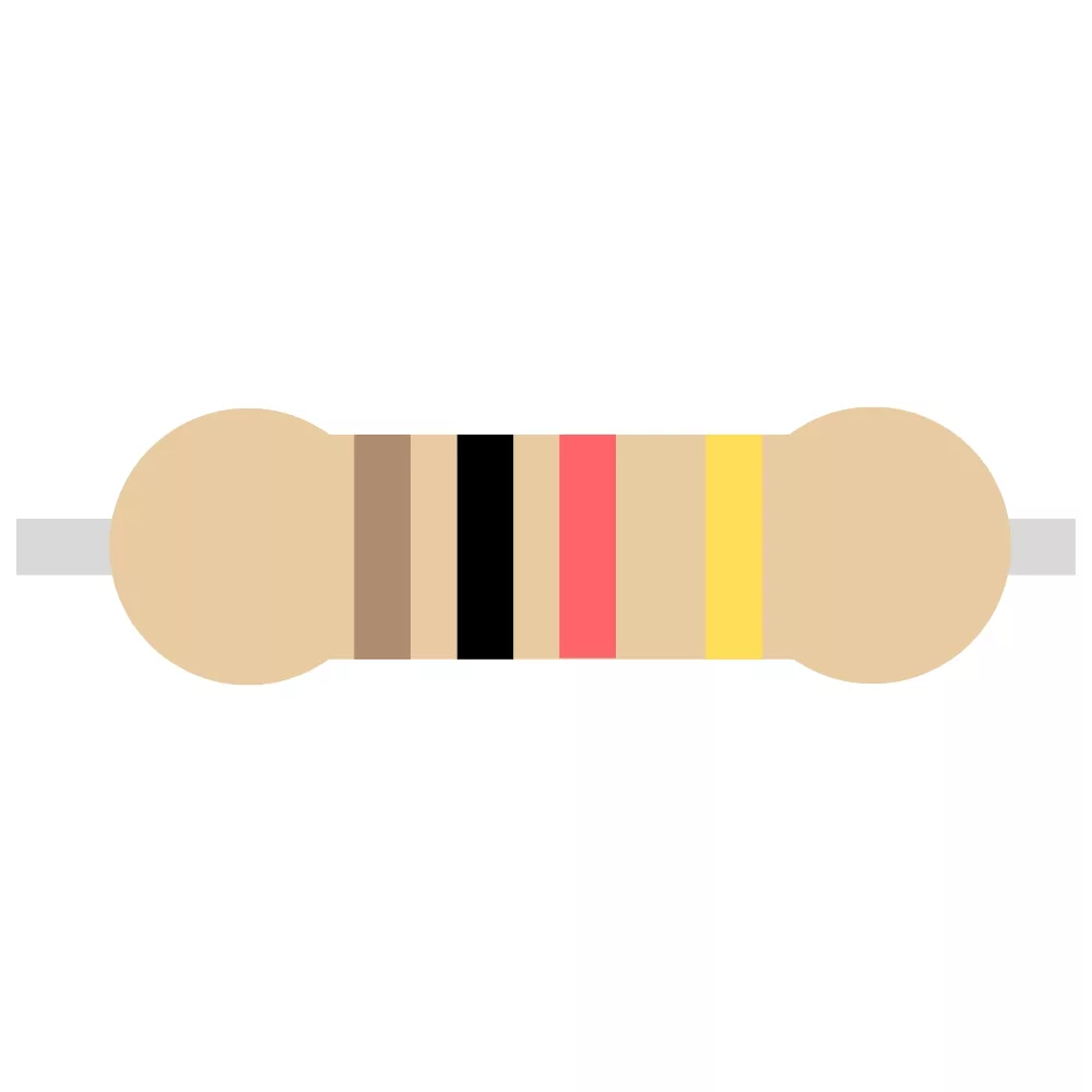 |
| 3mm Red LED | D1 - D6 | 6 | 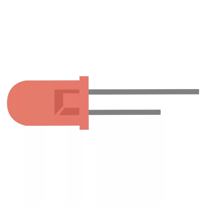 |
| Tactile Switch | SW1, SW2, SW4, SW5 | 4 | 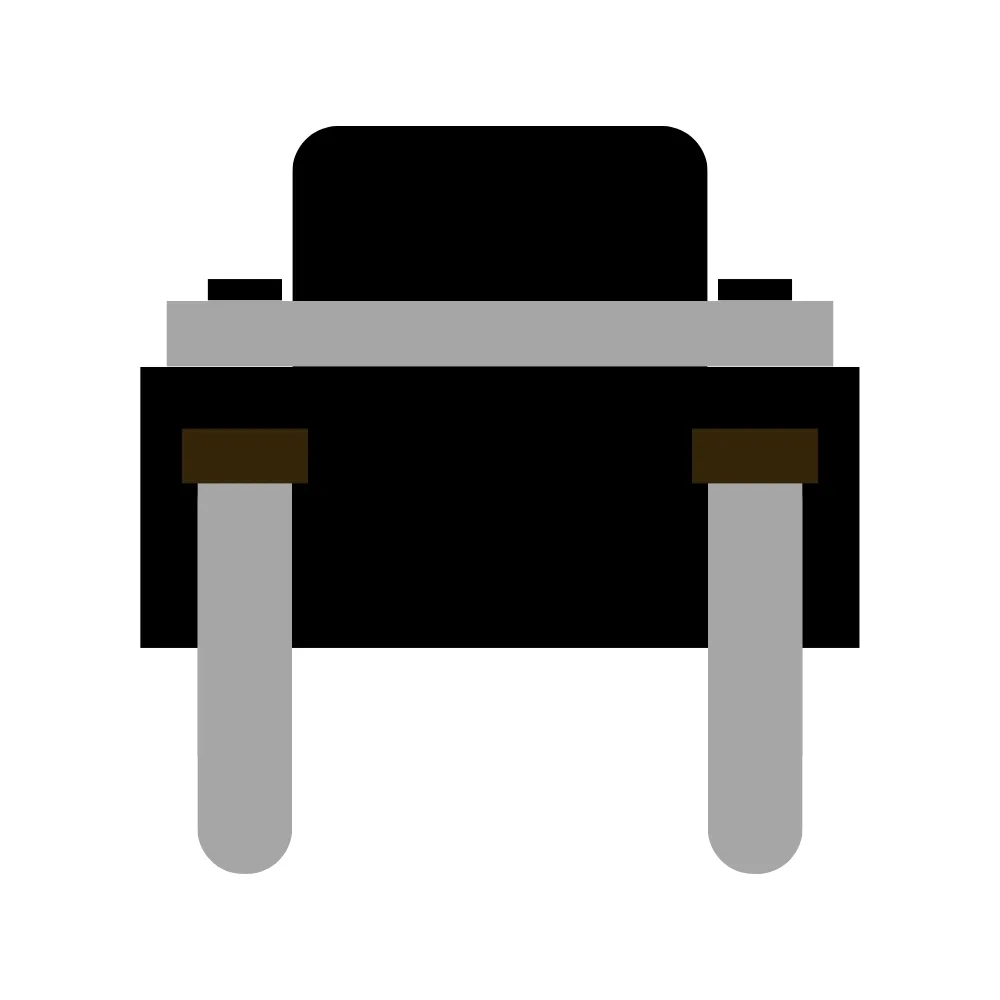 |
| Miniature Slide Switch | SW3 | 1 | 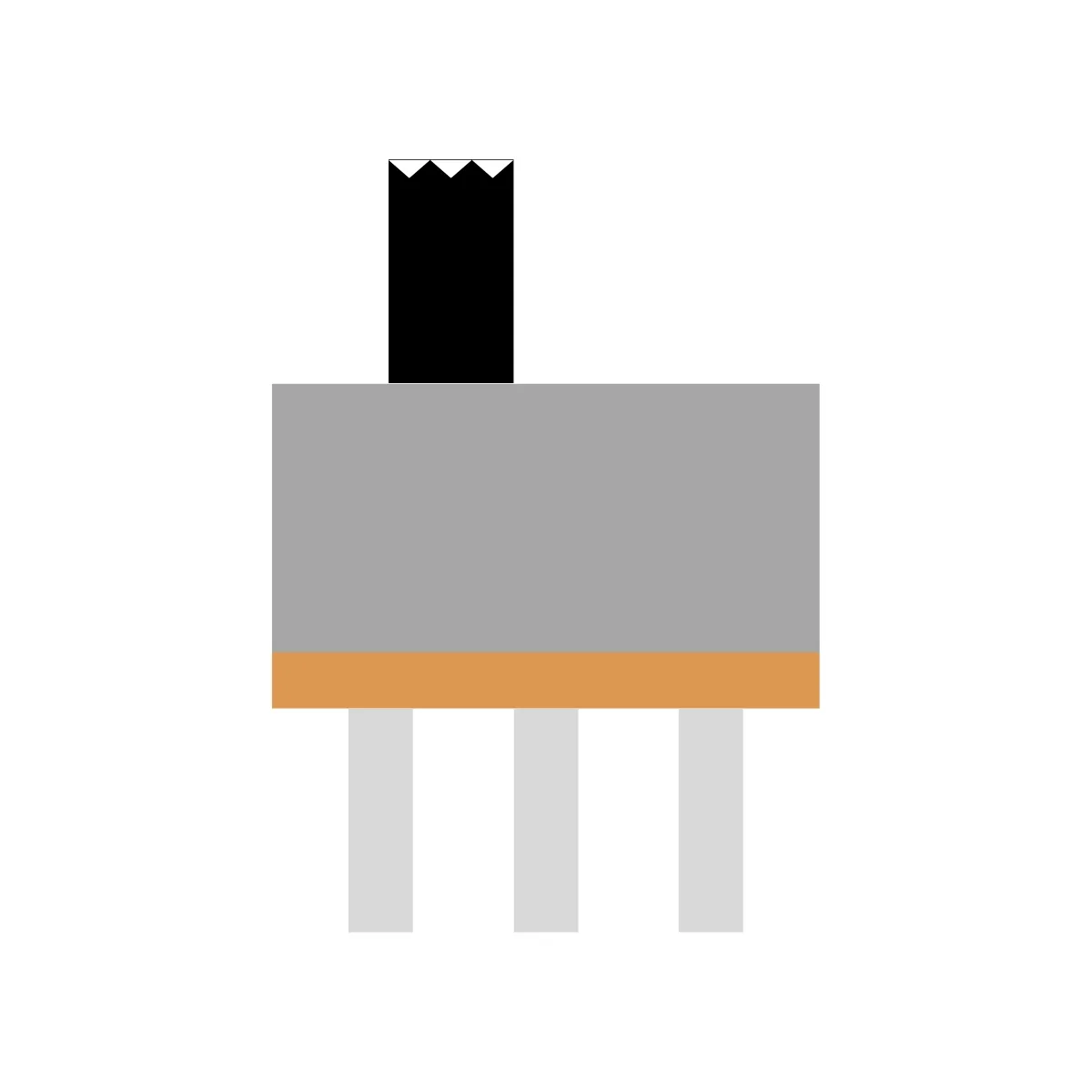 |
| PP3 Battery Connector | BT1 | 1 | 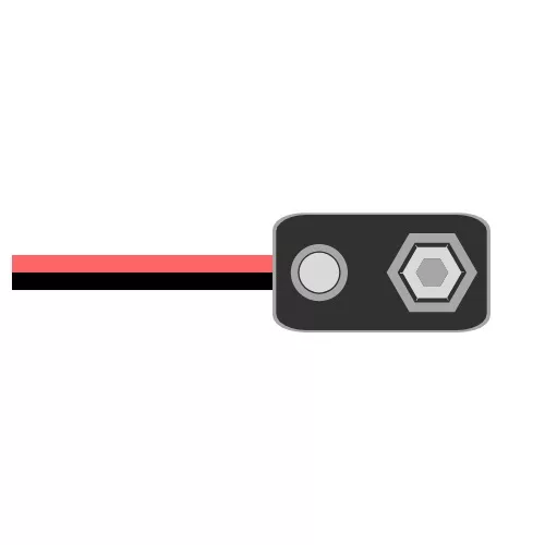 |
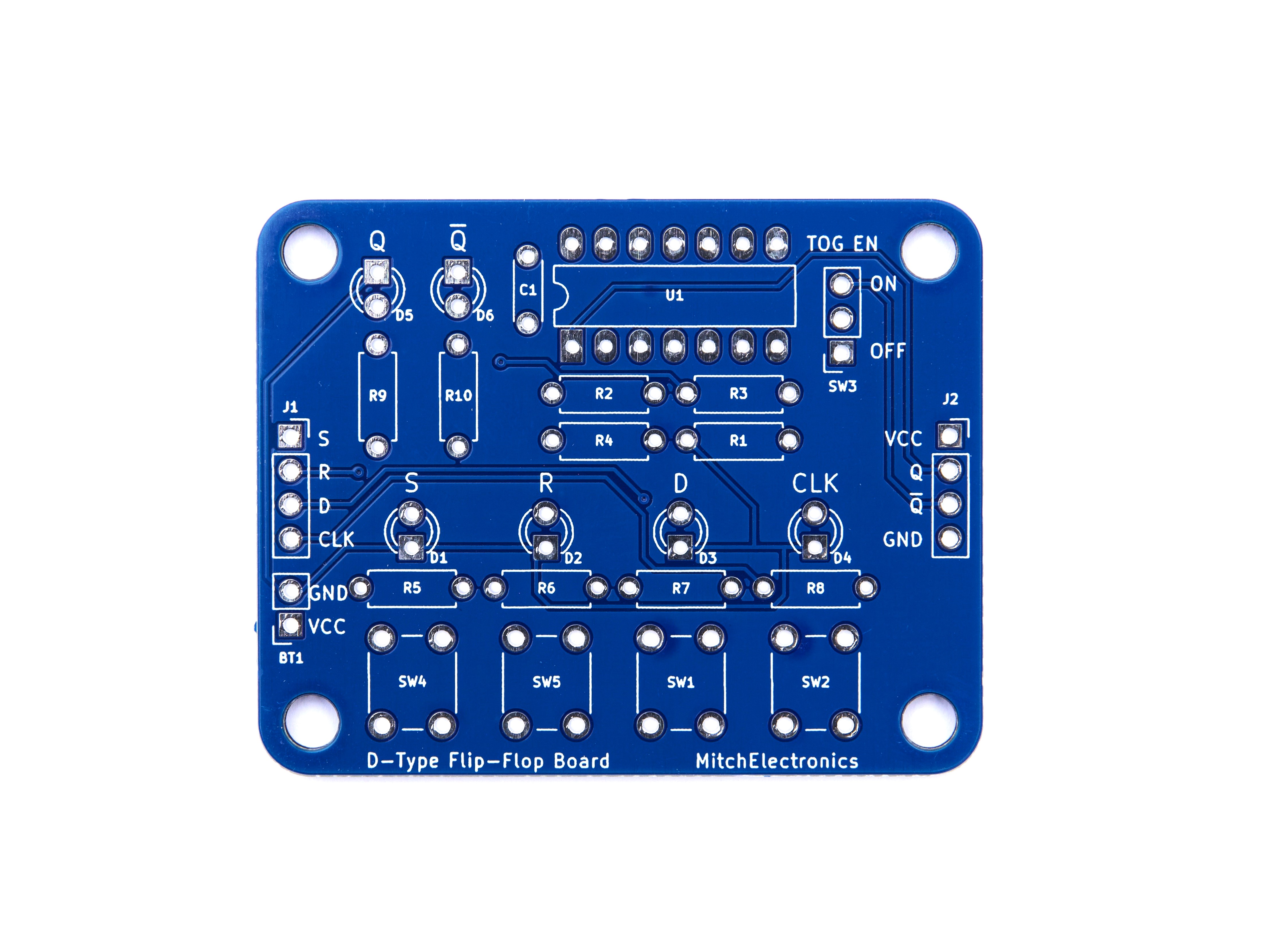
To learn more about how to solder electronic components, download the Electronics Construction Manual free using the button below
Electronics Construction Manual
When soldering components, it is essential that you do so in a particular order, so that it is easy to add components and get to their legs. Generally, you always start with the smaller components (such as resistors and capacitors), before moving onto the larget parts (potentiometers and ICs).
Soldering Guide
Use a signal generator to test how fast the logic circuits can respond to signals